Semiconductor fabrication is an intricate process that demands extreme precision at every stage, from lithography and etching to packaging and testing. Defects or inconsistencies at the microscale and nanoscale can significantly impact device performance, yield and reliability. Engineers and metrologists use advanced surface measurement techniques such as profilometry, scanning electron microscopy (SEM) and atomic force microscopy (AFM), coupled with specialized multi-modal analysis software to address the challenges they face.

A unified platform software
In semiconductor R&D and manufacturing environments, data is often generated using a variety of instruments and imaging techniques. Bringing together information from profilometers, SEMs, AFMs and other tools can be a challenge.
A unified analysis environment helps streamline this process, enabling engineers and researchers to interpret results more efficiently, compare findings across instrument technologies and make faster, data-driven decisions. Enter Mountains® software, a solution designed to support this type of cross-device analysis and help users gain a clearer understanding of complex surface structures.
Targeted tools for the semiconductor industry
Over the years, the Mountains® platform has built up an impressive set of dedicated solutions for semiconductor manufacturers working in wafer inspection, chip analysis and PCB assembly. These include tools for:
- Critical dimension analysis: characterization of trenches and nanometric structures in semiconductors with AFM and profilometry.
- Control of Line Edge Roughness (LER) and Line Width Roughness (LWR) to ensure uniformity in circuit patterns.
- Advanced topographical analysis to allow users to accurately calculate semiconductor surface flatness parameters.
- Through-silicon via (TSV) critical dimensioning to ensure uniformity of vias, a crucial factor for reliable electrical connectivity.
- Overlay measurement to detect misalignment between layers in semiconductor structures which can lead to device failure.
- High aspect ratio structure assessment (deep trenches, nano-pillars etc.)
- Edge detection: identification of holes, bumps and other structures, essential for detection of defects and process optimization.
- Analysis of thermal deformation of packaging to pinpoint issues with warpage.
- Automatic detection and analysis of step heights in semiconductor structures.
- Feature detection and pattern analysis to ensure compliance with design specifications.
- 3D reconstruction of SEM data to achieve deeper insights into nanoscale structures.
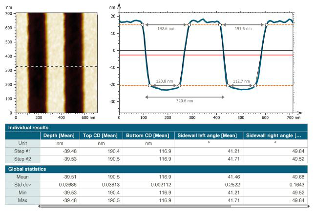
Above. Critical dimension analysis in semiconductor fabrication with AFM.
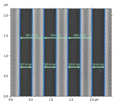
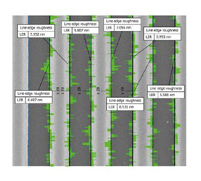
Above. Line edge roughness and deviation mapping on scanning electron microscope data.
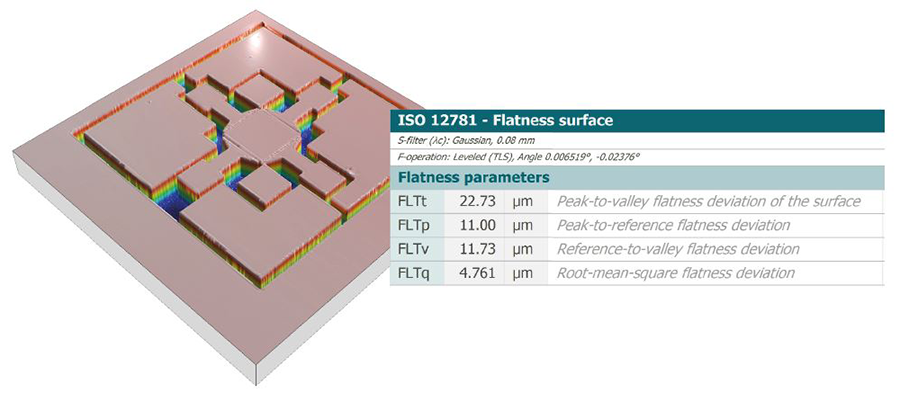
Above. Advanced topography analysis tools for semiconductor & MEMS surfaces including flatness parameters.
Automate your semiconductor workflow
Whether you are optimizing line roughness, verifying vias or analyzing step height variations, Mountains® software provides the added benefit of enabling you to easily automate your processes, thus dramatically reducing analysis time.
No-code automation tools for the semiconductor industry include:
- statistical documents, for identifying trends in large volumes of data
- automatic generation of analysis reports
- export of numerical data for processing with other statistical tools.
Stories (case studies)
- Optimizing critical dimension analysis in semiconductor fabrication with AFM
- Line Edge Roughness (LER) analysis for precision semiconductor characterization
- Analyzing silicon strain with Raman spectroscopy
- AFM image analysis: determining surface quality of cap layers in superconductors
- Analyzing data from a large-scale multi-instrument project
- Analyzing photoelectron spectroscopic measurements
- Semiconductors: characterizing 3D structures at the nanoscale
- Failure analysis in optoelectronic devices
Try Mountains® software for free
Try the tools out on your own semiconductor data