Newsletter
Stay up to-date with the latest imaging, analysis and metrology news from Digital Surf.
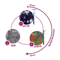
The AFM-IR lab at the Institute of Physical Chemistry, Paris-Saclay University (Orsay, France) is the pioneering research group in Infrared-Atomic Force Microscopy (AFM-IR). In particular, the team specializes in the characterization of complex materials, ranging from astro to biosciences, including studies on pathological calcifications such as breast microcalcifications (MCs), described in this article by Margaux Petay, former AFM-IR lab PhD student.
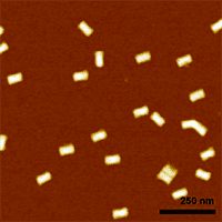
Simone Ruggeri, Associate Professor leading the Nanoscale Microscopy and Spectroscopy group at Wageningen University (WUR), Netherlands, tells us more about his current projects in the development of nano-analytical imaging and spectroscopic technologies to open a new research window of observation with nanoscale sensitivity in chemistry, biology and materials science.
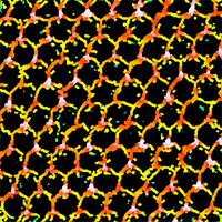
In the realm of dental implantology, understanding bacterial adhesion mechanisms is essential. Recent research led by Steve Papa and fellow researchers at the Jean Monnet University in Saint-Étienne, France, revealed the intricate relationship between surface topography and bacterial adhesion, with a particular focus on Porphyromonas gingivalis, a bacterium closely associated with dental implant failure.
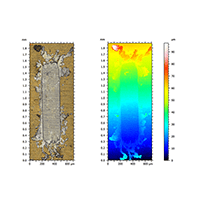
With the introduction of the new Color segmentation tool in Mountains® software, it is now possible to complement topographical wear analysis. Mathieu Cognard, product manager at Digital Surf, explains how MountainsImage® can help visualize & analyze your results.
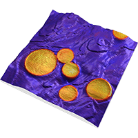
In the last few years, the use of SPM techniques in many areas of research has greatly increased. Professor Philippe Leclere, director of the LPNE at the University of Mons (UMONS) in Belgium, has been studying the impact of this increase and describes how his team is addressing the challenge of analyzing and mapping large quantities of data on material properties at the nanoscale.
Strain in semiconductor devices can be used to influence the electronic properties, and is used as so in strain engineering. Renata Lewandowska, product manager for spectral applications at Digital Surf, explains why Raman spectroscopy is an ideal technique for measuring strain, and give us an example.
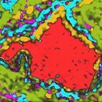
Application experts at Horiba Scientific and JEOL Europe recently highlighted a technique for precisely relocalizing specific areas of a sample for analysis using various techniques including Raman microscopy, scanning electron microscopy (SEM) and energy dispersive spectroscopy (EDS).
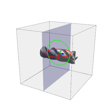
One of the critical applications of optical metrology in tooling is the dimensional characterization of cutting tools. Roughness measurements can also be used to predict how removed material will exit the tool in the aim of preventing clot formation or overheating. In addition, optical metrology can provide local measurements to help identify issues such as chipping or coating peeling, which indicate if a tool needs to be replaced or repaired. In this study, all these characterizations were managed using one, unique set-up: the Sensofar S neox Five Axis and SensoMap software powered by Mountains®.
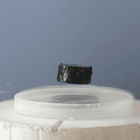
Researchers at the Institut de Ciència de Materials de Barcelona characterizied surface texture of superconductor materials with the aim of improving their performance.
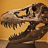
Dr. Mugino O. Kubo Ph.D at the University of Tokyo, Japan speaks about how her team are using three-dimensional microwear analysis and implementing new methods for studying the paleodiet of carnivorous dinosaurs, including the iconic Tyrannosaurus rex.
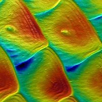
Researchers at Purdue and Harvard universities explored fish scale surfaces in 3D using MountainsMap® software.
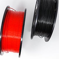
A team at Widener University (Chester, Pennsylvania, USA) recently used bimodal AFM technique and MountainsSPIP® software to study the calcification process of polylactic acid polymer (PLA), a plastic filament material widely used in 3D printing.