Semiconductor designers are constantly pushing back the limits of materials science. In the current age of the atomic-level device, one of the main challenges for researchers is to characterize the performance and properties of structures at the nanoscale.
Bruno Grandidier, research scientist with the French National Center for Scientific Research (CNRS), reports on his work, focused on understanding the electronic properties of silicon dangling bonds.
“Silicon adopts the diamond crystal structure displayed by carbon and thus forms tetrahedral sp3 bonds.
At the surface of a Si crystal, the periodicity of the crystal is broken and the surface atoms rearrange themselves to diminish the number of unsatisfied bonds. These non-bonding sp orbitals, which are localized on three-fold-coordinated Si atoms, are known as dangling bonds. While they had an undesirable effect on electronic devices in the past, they are now regarded as the ultimate quantum dot for engineering quantum devices on silicon surfaces1.”
A flower-like shape on the crystal surface
“Non-passivated dangling bonds can be created on a the surface of a Si(111) crystal that is highly doped with boron atoms to yield a B-doped Si(111)-√3x√3R30° surface. They give rise to localized states in the band gap of silicon (1.2 eV) that can be characterized with scanning tunneling microscopy (STM) and spectroscopy at a single level.
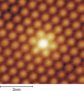
In the atomically-resolved STM image below, each rounded protrusion corresponds to a single Si adatom (atom lying on the crystal surface). A non-passivated dangling bond appears as a very bright adatom, surrounded by six bright adatom neighbors, forming a flower-like shape.”

“By acquiring spatial maps of the current and the differential conductivity along with the topography (using a method called Current Imaging Tunneling Spectroscopy or CITS), it is possible to measure the extent of the electron wave function of each quantum level of the non-passivated dangling bond with picometer resolution2&3.”
References
1. Schofield, S. R., et al. “Quantum engineering at the silicon surface using dangling bonds.” Nature communications 4 (2013): 1649.
2. Berthe, M., et al. “Probing the carrier capture rate of a single quantum level.” Science 319.5862 (2008): 436-438.
3. Nguyen, T. H., et al. “Coulomb energy determination of a single Si dangling bond.” Physical review letters 105.22 (2010): 226404.
Mountains® tools used
Mountains® software was used to view and analyze CITS cubes containing 14,400 spectra. The search for localized states and the visualization of the spatial distribution of the electron on each state was achieved either manually or automatically, thanks to two recently developed tools.
1- Sort spectra
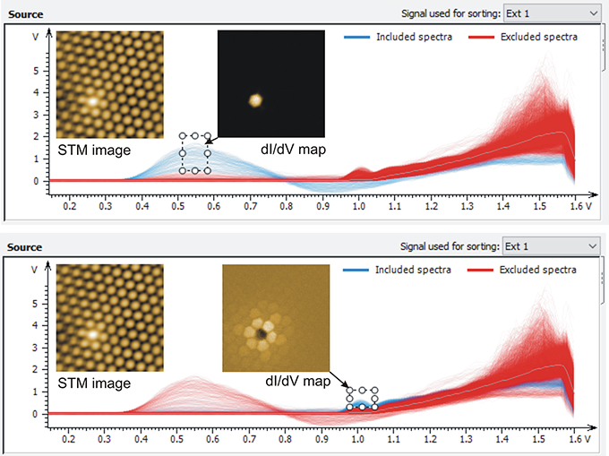
The first is based on the selection of a set of spectra from a flattened spectra view. As shown below, the flattened spectra view allows direct observation of peaks and of their spatial occurrence using the Sort spectra operator. The results are then compared to the topography and the extracted slices of the dI/dV cube (see insets) at a particular energy peak in order to determine the energy level properties.

Above: Flattened spectra view helps determine energy level properties
2- Extract component
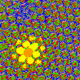
The second method relies on powerful algorithms for independent component analysis (ICA), to demix a set of statistically independent sources (orthogonal quantum states). As shown in the figure below, the Extract component operator provides robust data mining capabilities for spatial mapping of both quantum levels. Moreover, for each component detected, the operator indicates the related spectrum, thus simplifying the screening of large numbers of spectra.

Above: Result of component extraction
Results
The study reveals the existence of two states, one level positioned deep in the band gap of silicon and strongly localized on the Si adatom and a second level below the edge of the conduction band with a spatial extent over a few Si adatom neighbors. Such analysis is of great importance in understanding electron transfer dynamics and the Coulomb repulsion into a single Si orbital as well as the interaction of the electron with the vibrational modes of the Si adatom.
Instrument & software used
Current Imaging Tunneling Spectroscopy (CITS) + MountainsSPIP® + Spectroscopy module