The semiconductor industry, today’s driving force behind modern technology, relies on uncompromised metrological precision. The quality and performance of devices closely depend on the accuracy with which the critical dimensions (CD) of nanometric structures are measured and analyzed.
In this context, atomic force microscopy (AFM) has become an indispensable technique, capable of providing detailed information on surface topography at the nanoscale. However, the optimal exploitation of AFM data requires powerful and adapted software, capable of transforming raw data into actionable insights. This is where Digital Surf’s Mountains® software comes into play, offering a comprehensive and high-performance solution for the precise and efficient analysis of CDs in the semiconductor field.
Precise calculations of critical dimensions
Characterizing trenches and complex structures of semiconductors presents a significant challenge. Measurement precision is paramount, as the exact determination of step height, top & bottom width, sidewall angles and pitch directly influence the quality and reliability of devices.
Mountains® software provides dedicated tools for CD analysis, ensuring precise determination of critical parameters, such as roughness, curvature and structural dimensions.
An AFM image of a waveguide pattern and the corresponding CD analysis is shown in Figure 1. The critical dimensions measured in this example were the mean trench depth, width and sidewall angles along two motifs. The pitch was also determined automatically between two trenches.
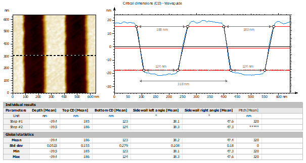
Figure 1 Critical dimensions analysis of a waveguide – Determination of trench depth and width, sidewall angles and pitch.
Automation of CD analysis
The massive volume of data generated by AFM requires powerful analysis tools, capable of rapidly processing and interpreting information. Mountains® software addresses these challenges with a range of features designed to optimize each step of the analysis workflow than can be automated in order to batch process datasets.
Surface roughness analysis in silicon photonics
For the characterization and optimization of patterned silicon, especially within silicon photonics applications, surface roughness analysis complements critical dimension measurements.
High roughness values in these devices induce light scattering, negatively impacting efficiency. A sample containing silicon and photoresist must thus demonstrate low roughness values, specifically with an Sq value below 1 nm, with silicon expected to be the smoother component. In figure 2, the analysis shows that silicon is smoother, as expected, with a roughness (Sq) of 0.480 nm versus 0.756 nm for the photoresist. Topographical analysis indicates roughness anomalies inconsistent with polished silicon, potentially attributable to presence of a contaminant.
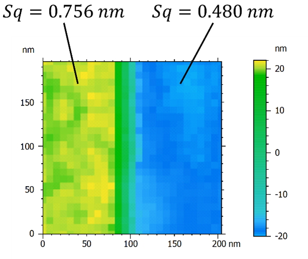
Figure 2 Surface roughness characterization of a silicon/photoresist composite sample.
Advanced features for bulk data analysis & compliance
Mountains® software also offers advanced features for statistical data analysis, allowing for the identification of trends and variations, thus ensuring rigorous quality control.
The generation of customized reports facilitates the documentation and communication of results, this being a crucial aspect in the semiconductor industry, where traceability and compliance with standards are paramount.
Instrument & software used
Atomic Force Microscope & MountainsSPIP® software