In the last few years, the use of SPM techniques in many areas of research has greatly increased. Professor Philippe Leclere, director of the Laboratory for Physics of Nanomaterials and Energy (LPNE) at the University of Mons (UMONS) in Belgium, within the Research Institute for Materials Science and Engineering, has been studying the impact of this increase and describes how his team is addressing the challenge of analyzing and mapping large quantities of data on material properties at the nanoscale.

Scanning Probe Microscopy (SPM) is one of the main tools responsible for the emergence of novel soft functional materials and for the characterization of their physical properties at the nanoscale.
Big data issues in SPM
At the Laboratory for Physics of Nanomaterials and Energy (LPNE), SPM helps us to solve various challenges we face with materials in the fields of energy harvesting, organic electronics, biosensors, self-assembly, biotechnology, life sciences, and nanomedicine to name but a few.
The number of advanced SPM techniques commercially available these days keeps growing at an extremely fast rate and this generates a huge amount of data.
The quantitative mapping of the actual mechanical properties of materials at the nanoscale constitutes a real challenge for professionals.
The number of collected observables is also rapidly increasing and machine learning processes are now mature enough to analyze data user-independently. Most of the existing imaging modes proposed by the manufacturers take into account one of the contact mechanical models (among the few analytically available) for the entire acquisition.

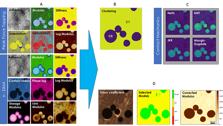
Figure 1. Andy Warhol-like representation of the data analysis of PS-PCL polymer blend. Panel A. Each image represents one of the observables (or material properties) obtained by PFT or n-DMA. Panel B. Results of the data clustering (here k = 2). Panel C. Rigidity modulus map calculations depending on the contact mechanics model used. Panel D. Calculated Tabor coefficient map, the selected model and the re-mapping of the rigidity modulus according to the most appropriate model.
Recalculating rigidity modulus on PS-PCL
In this growing field of research, the contribution of the LPNE mainly consists of data clustering and mapping of material properties using the most appropriate contact mechanics model for each pixel based on the approach–retract force curve analysis.
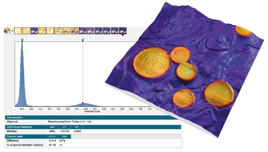
We were able to recalculate the mechanical properties such as the rigidity modulus with the aim of importing all these channels into MountainsSPIP® software for deeper analysis, particularly statistical analysis, and to benefit from the software’s rendering capacities.
Figure 1 illustrates the capabilities of this approach on a polymer blend made of polystyrene (30%) and polycaprolactone (70%) using Peak Force Tapping (PFT) and nano Dynamic Mechanical Analysis (n-DMA) techniques. The polystyrene (PS) forms circular-shaped objects within the semi-crystalline matrix of the polycaprolactone (PCL).
This process has been extended with success to many other materials including nanocomposites, hydrogels, block copolymers, cosmetics and bacteria.
For the data clustering process, it is important to emphasize that any channel corresponding to electrical, magnetic, thermal or piezoelectrical properties can be considered as an input observable, thus extending the analysis to any material property.
For this purpose, we used Principal Component Analysis, K-Means or Gaussian Mixed Model algorithms.

Figure 2. Recalculated rigidity modulus histogram (left) and 3D visualization of the recalculated modulus overlaid on a the corresponding topography channel (right).
Contact
Professor Philippe Leclere – philippe.leclere@umons.ac.be – @LpneUmons
Instruments & software used
Scanning probe microscope (Bruker Dimension Icon) and MountainsSPIP® 10 software